FILTERS

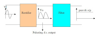
FILTERSWe know that the output of the rectifier is pulsating d.c. ie the output obtained by the rectifier is not pure d.c. but it contains some ac components along with the dc o/p. These ac components are called as Ripples, which are undesirable or unwanted. To minimize the ripples in the rectifier output filter circuits are used. These circuits are normally connected between the rectifier and load as shown below.

Filter is a circuit which converts pulsating dc output from a rectifier to a steady dc output. In otherwords, filters are used to reduce the amplitudes of the unwanted ac components in the rectifier.

Note: A capacitor passes ac signal readily but blocks dc.

Types of Filters

1. Capacitor Filter (C-Filter)
2. Inductor Filter
3. Choke Input Filter (LC-filter)
4. Capacitor Input Filter (Π-filter)

Capacitor Filter( C-filter)

• When the Input signal rises from o to a the diode is forward biased therefore it starts conducting since the capacitor acts as a short circuit for ac signal it gets charged up to the peak of the input signal and the dc component flows through the load RL.

• When the input signal fall from a to b the diode gets reverse biased . This is mainly because of the voltage across the capacitor obtained during the period o to a is more when comapared to Vi. Therefore there is no conduction of current through the diode.

• Now the charged capacitor acts as a battery and it starts discharging through the load RL. Mean while the input signal passes through b,c,d section. When the signal reaches the point d the diode is still reverse biased since the capacitor voltage is more than the input voltage.

• When the signal reaches point e, the input voltage can be expected to be more than the capacitor voltage. When the input signal moves from e to f the capacitor gets charged to its peak value again. The diode gets reverse biased and the capacitor starts discharging. The final output across RL is shown in Fig.

Advantages of C-Filter

• low cost, small size and good characteristics.
• It is preferred for small load currents ( upto 50 mA)
• It is commonly used in transistor radio, batteries eliminator etc.


RECTIFIERS

RECTIFIERS

“Rectifiers are the circuit which converts ac to dc”

Rectifiers are grouped into tow categories depending on the period of conductions.
1. Half-wave rectifier
2. Full- wave rectifier.

Half-wave rectifier
The circuit diagram of a half-wave rectifier is shown in fig below along with the I/P and O/P waveforms.

Half wave rectifier (i) Circuit diagram (ii) waveforms

• The transformer is employed in order to step-down the supply voltage and also to prevent from shocks.

• The diode is used to rectify the a.c. signal while , the pulsating d.c. is taken across the load resistor RL.

• During the +ve half cycle, the end X of the secondary is +ve and end Y is -ve . Thus , forward biasing the diode. As the diode is forward biased, the current flows through the load RL and a voltage is developed across it.

• During the –ve half-cycle the end Y is +ve and end X is –ve thus, reverse biasing the diode. As the diode is reverse biased there is no flow of current through RL thereby the output voltage is zero.

Full-wave rectifier

Full-wave rectifier are of two types

1. Centre tapped full-wave rectifier
2. Bridge rectifier

Centre tapped full –wave rectifier

Centre tapped Full wave rectifier (i) Circuit diagram (ii) waveforms

• The circuit diagram of a center tapped full wave rectifier is shown in fig. 2.6 above. It employs two diodes and a center tap transformer. The a.c. signal to be rectified is applied to the primary of the transformer and the d.c. output is taken across the load RL.

• During the +ve half-cycle end X is +ve and end Y is –ve this makes diode D1 forward biased and thus a current i1 flows through it and load resistor RL.Diode D2 is reverse biased and the current i2 is zero.
• During the –ve half-cycle end Y is +Ve and end X is –Ve. Now diode D2 is forward biased and thus a current i2 flows through it and load resistor RL. Diode D1 is reversed and the current i1 = 0.
Disadvantages

• Since, each diode uses only one-half of the transformer secondary voltage the d.c. output is comparatively small.
• It is difficult to locate the center-tap on secondary winding of the transformer.
• The diodes used must have high Peak-inverse voltage.

Bridge rectifier

Full wave bridge wave rectifier (i) Circuit diagram (ii) waveforms.

• The circuit diagram of a bridge rectifer is shown above. It uses four diodes and a transformer.

• During the +ve half-cycle, end A is +ve and end B is –ve thus diodes D1 and D3 are forward bias while diodes D2 and D4 are reverse biased thus a current flows through diode D1, load RL ( C to D) and diode D3.

• During the –ve half-cycle, end B is +ve and end A is –ve thus diodes D2 and D4 are forward biased while the diodes D1 and D3 are reverse biased. Now the flow of current is through diode D4 load RL ( D to C) and diode D2. Thus, the waveform is same as in the case of center-tapped full wave rectifier.
Advantages

• The need for center-taped transformer is eliminated.
• The output is twice when compared to center-tapped full wave rectifier.
for the same secondary voltage.
• The peak inverse voltage is one-half(1/2) compared to center-tapped full wave rectifier.
• Can be used where large amount of power is required.

Disadvantages

• It requires four diodes.
• The use of two extra diodes cause an additional voltage drop thereby reducing the output voltage.

Basic Definitions

Basic Definitions

1.Knee voltage or Cut-in Voltage.
It is the forward voltage at which the diode starts conducting.

2. Breakdown voltage
It is the reverse voltage at which the diode (p-n junction) breaks down with sudden rise in reverse current.

3. Peak-inverse voltage (PIV)
It is the max. reverse voltage that can be applied to a p-n junction without causing damage to the junction.

If the reverse voltage across the junction exceeds its peak-inverse voltage, then the junction exceeds its Peak-inverse voltage, then the junction gets destroyed because of excessive heat. In rectification, one thing to be kept in mind is that care should be taken that reverse voltage across the diode during –ve half cycle of a.c. doesnot exceed the peak-inverse voltage of the diode.

4. Maximum Forward current
It is the Max. instantaneous forward current that a p-n junction can conduct without damaging the junction. If the forward current is more than the specified rating then the junction gets destroyed due to over heating.

5.Maximum Power rating
It is the maximum power that can be dissipated at the junction without damaging it. The power dissipated across the junction is equal to the product of junction current and the voltage across the junction.

Volt- Ampere characteristics(V-I)

V-I characteristics of p-n junction diode.
(i) Circuit diagram
(ii) Characteristics

• The V-I characteristics of a semiconductor diode can be obtained with the help of the circuit shown in fig.

• The supply voltage V is a regulated power supply, the diode is forward biased in the circuit shown. The resistor R is a current limiting resistor. The voltage across the diode is measured with the help of voltmeter and the current is recorded using an ammeter.

• By varying the supply voltage different sets of voltage and currents are obtained. By plotting these values on a graph, the forward characteristics can be obtained. It can be noted from the graph the current remains zero till the diode voltage attains the barrier potential.

• For silicon diode, the barrier potential is 0.7 V and for Germanium diode, it is 0.3 V. The barrier potential is also called as knee voltage or cur-in voltage.

• The reverse characteristics can be obtained by reverse biasing the diode. It can be noted that at a particular reverse voltage, the reverse current increases rapidly. This voltage is called breakdown voltage.


SEMICONDUCTOR DIODE

SEMICONDUCTOR DIODE

When a p-type semiconductor material is suitably joined to n-type semiconductor the contact surface is called a p-n junction. The p-n junction is also called as semiconductor diode.
• The left side material is a p-type semiconductor having –ve acceptor ions and +vely charged holes. The right side material is n-type semiconductor having +ve donor ions and free electrons.

• Suppose the two pieces are suitably treated to form pn junction, then there is a tendency for the free electrons from n-type to diffuse over to the p-side and holes from p-type to the n-side . This process is called diffusion.


• As the free electrons move across the junction from n-type to p-type, +ve donor ions are uncovered. Hence a +ve charge is built on the n-side of the junction. At the same time, the free electrons cross the junction and uncover the –ve acceptor ions by filling in the holes. Therefore a net –ve charge is established on p-side of the junction.

• When a sufficient number of donor and acceptor ions is uncovered further diffusion is prevented.


• Thus a barrier is set up against further movement of charge carriers. This is called potential barrier or junction barrier Vo. The potential barrier is of the order of 0.1 to 0.3V.

Note: outside this barrier on each side of the junction, the material is still neutral. Only inside the barrier, there is a +ve charge on n-side and –ve charge on p-side. This region is called depletion layer.

2.1 Biasing: Connecting a p-n junction to an external d.c. voltage source is called
biasing.

1. Forward biasing
2. Reverse biasing

1. Forward biasing

• When external voltage applied to the junction is in such a direction that it cancels the potential barrier, thus permitting current flow is called forward biasing.

• To apply forward bias, connect +ve terminal of the battery to p-type and –ve terminal to n-type as shown in fig.2.1 below.


• The applied forward potential establishes the electric field which acts against the field due to potential barrier. Therefore the resultant field is weakened and the barier height is reduced at the junction as shown in fig. 2.1.

• Since the potential barrier voltage is very small, a small forward voltage is sufficient to completely eliminate the barrier. Once the potential barrier is eliminated by the forward voltage, junction resistance becomes almost zero and a low resistance path is established for the entire circuit. Therefore current flows in the circuit. This is called forward current.2. Reverse biasing

• When the external voltage applied to the junction is in such a direction the potential barrier is increased it is called reverse biasing.

• To apply reverse bias, connect –ve terminal of the battery to p-type and +ve terminal to n-type as shown in figure below.

• The applied reverse voltage establishes an electric field which acts in the same direction as the field due to potential barrier. Therefore the resultant field at the junction is strengthened and the barrier height is increased as shown in fig.

• The increased potential barrier prevents the flow of charge carriers across the junction. Thus a high resistance path is established for the entire circuit and hence current does not flow.

HALL EFFECT

HALL EFFECT


If a piece of metal or semiconductor carrying a current I is placed in a transverse magnetic field B then an electric field E is induced in the direction perpendicular to both I and B. This phenomenon is known as Hall effect.

Hall effect is normally used to determine whether a semi-conductor is n-type or p-type.

To find whether the semiconductor is n-type or p-type

i) In the figure. above, If I is in the +ve X direction and B is in the +ve Z direction, then a force will be exerted on the charge carriers (holes and electrons) in the –ve Y direction.

ii) This force is independent of whether the charge carriers are electrons or holes. Due to this force the charge carriers ( holes and electrons) will be forced downward towards surface –1 as shown.

iii) If the semiconductor is N-type, then electrons will be the charge carriers and these electrons will accumulate on surface –1 making that surface –vely charged with respect to surface –2. Hence a potential called Hall voltage appears between the surfaces 1 and 2.

iv) Similarly when surface –1 is positively charged with respect to surface –2, then the semiconductor is of P-type. In this way, by seeing the polarity of Hall voltage we can determine whether the semiconductor is of P-type or N-type.

Applications of Hall effect

Hall effect is used to determine,

• carrier concentration, conductivity and mobility.
• The sign of the current carrying charge.
• Charge density.
• It is used as magnetic field meter.

Carrier lifetime (τ)

In a pure semiconductor, we know that number of holes are equal to the number of electrons. Thermal agitation however, continues to produce new hole electron pairs while other hole-electron pair disappear as a result of recombination.

On an average, a hole will exist for τp second and an electron will exist for τn second before recombination. This time is called the carrier lifetime or Mean lifetime.

The average time an electron or hole can exist in the free state is called carrier lifetime.

Fermi-level

Fermi-level

Fermi level indicates the level of energy in the forbidden gap.

1. Fermi-level for an Intrinsic semiconductor

• We know that the Intrinsic semiconductor acts as an insulator at absolute zero temperature because there are free electrons and holes available but as the temperature increases electron hole pairs are generated and hence number of electrons will be equal to number of holes.

• Therefore, the possibility of obtaining an electron in the conduction band will be equal to the probability of obtaining a hole in the valence band.

• If Ec is the lowest energy level of Conduction band and Ev is the highest energy level of the valence band then the fermi level Ef is exactly at the center of these two levels as shown above.

2. Fermi-level in a semiconductors having impurities (Extrinsic)

a) Fermi-level for n-type Semiconductor

• Let a donar impurity be added to an Intrinsic semiconductor then the donar energy level (ED) shown by the dotted lines is very close to conduction band energy level (Ec).

• Therefore the unbonded valence electrons of the impurity atoms can very easily jump into the conduction band and become free electros thus, at room temperature almost all the extra electrons of pentavalent impurity will jump to the conduction band.

• The donar energy level (ED) is just below conduction band level (Ec) as shown in figure. Due to a large number of free electrons, the probability of electrons occupying the energy level towards the conduction band will be more hence, fermi level shifts towards the conduction band.b) Fermi-level for P-type semiconductor

• Let an acceptor impurity be added to an Intrinsic semiconductor then the acceptor energy level (Ea) shown by dotted lines is very close to the valence band shown by dotted lines is very close to the valence band energy level (Ev).

• Therefore the valence band electrons of the impurity atom can very easily jump into the valence band thereby creating holes in the valence band.

• The acceptor energy level (EA) is just above the valence band level as shown in figure.

• Due to large number of holes the probability of holes occupying the energy level towards the valence band will be more and hence, the fermi level gets shifted towards the valence band.


Drift and Diffusion current

Drift and Diffusion current


The flow of current through a semiconductor material is normally referred to as one of the two types.


Drift current
• If an electron is subjected to an electric field in free space it will accelerate in a straight line form the –ve terminal to the + ve terminal of the applied voltage.

• However in the case of conductor or semiconductor at room temperature, a free electrons under the influence of electric field will move towards the +ve terminal of the applied voltage but will continuously collide with atoms all the ways as shown in figure
• Each time, when the electron strikes an atom, it rebounds in a random direction but the presence of electric field doesnot stop the collisions and random motion. As a result the electrons drift in a direction of the applied electric field.

• The current produced in this way is called as Drift current and it is the usual kind of current flow that occurs in a conductor.

Diffusion current

• The directional movement of charge carriers due to their concentration gradient produces a component of current known as Diffusion current.

• The mechanism of transport of charges in a semiconductor when no electric field is applied called diffusion. It is encountered only in semiconductors and is normally absent in conductors.
• With no applied voltage if the number of charge carriers (either holes or electrons) in one region of a semiconductor is less compared to the rest of the region then there exist a concentration gradient.

• Since the charge carriers are either all electrons or all holes they sine polarity of charge and thus there is a force of repulsion between them.

• As a result, the carriers tend to move gradually or diffuse from the region of higher concentration to the region of lower concentration. This process is called diffusion and electric current produced due to this process is called diffusion current.

• This process continues until all the carriers are evenly distributed through the material. Hence when there is no applied voltage, the net diffusion current will be zero.


p-type semiconductor


p-type semiconductor

• When a small amount of trivalent impurity is added to a pure semiconductor it is called p-type semiconductor.

• The addition of trivalent impurity provides large number of holes in the semiconductor crystals.

• Example: Gallium, Indium or Boron etc. Such impurities which produce p-type semiconductors are known as acceptor impurities because the holes created can accept the electrons in the semi conductor crystal.

To understand the formation of p-type semiconductor, consider a pure silicon crystal with an impurity say gallium added to it as shown in figure 1.7.

• We know that silicon atom has 4 valence electrons and Gallium has 3 electrons. When Gallium is added as impurity to silicon, the 3 valence electrons of gallium make 3 covalent bonds with 3 valence electrons of silicon.

• The 4th valence electrons of silicon cannot make a covalent bond with that of Gallium because of short of one electron as shown above. This absence of electron is called a hole. Therefore for each gallium atom added one hole is created, a small amount of Gallium provides millions of holes.

Due to thermal energy, still hole-electron pairs are generated but the number of holes are very large compared to the number of electrons. Therefore, in a p-type semiconductor holes are majority carriers and electrons are minority carriers. Since the current conduction is predominantly by hole( + charges) it is called as p-type semiconductor( p means +ve)

N-Type semiconductor

N-Type semiconductor

  • When a small current of Pentavalent impurity is added to a pure semiconductor it is called as n-type semiconductor.

  • Addition of Pentavalent impurity provides a large number of free electrons in a semiconductor crystal.

  • Typical example for pentavalent impurities are Arsenic, Antimony and Phosphorus etc. Such impurities which produce n-type semiconductors are known as Donor impurities because they donate or provide free electrons to the semiconductor crystal.

To understand the formation of n-type semiconductor, consider a pure silicon crystal with an impurity say arsenic added to it as shown in figure

  • We know that a silicon atom has 4 valence electrons and Arsenic has 5 valence electrons. When Arsenic is added as impurity to silicon, the 4 valence electrons of silicon make co-valent bond with 4 valence electrons of Arsenic.

  • The 5th Valence electrons finds no place in the covalent bond thus, it becomes free and travels to the conduction band as shown in figure. Therefore, for each arsenic atom added, one free electron will be available in the silicon crystal. Though each arsenic atom provides one free electrons yet an extremely small amount of arsenic impurity provides enough atoms to supply millions of free electrons.


Due to thermal energy, still hole election pairs are generated but the number of free electrons are very large in number when compared to holes. So in an n-type semiconductor electrons are majority charge carriers and holes are minority charge carriers . Since the current conduction is pre-dominantly by free electrons( -vely charges) it is called as n-type semiconductor( n- means –ve).


Classification of semiconductors

Semiconductors are classified into two types.

a) Intrinsic semiconductors.

b) Extrinsic semiconductors.

a) Intrinsic semiconductors

· A semiconductor in an extremely pure form is known as Intrinsic semiconductor.

Example: Silicon, germanium.

· Both silicon and Germanium are tetravalent (having 4 valence electrons).

· Each atom forms a covalent bond or e

lectron pair bond with the electrons of neighboring atom. The structure is shown below.

At low temperature

  • At low temperature, all the valence electrons are tightly bounded the nucleus hence no free electrons are available for conduction.

  • The semiconductor therefore behaves as an Insulator at absolute zero temperature.

At room temperature

  • At room temperature, some of the valence electrons gain enough thermal energy to break up the covalent bonds.

  • This breaking up of covalent bonds sets the electrons free and are available for conduction.

  • When an electron escapes from a covalent bond and becomes free electrons a vacancy is created in a covalent bond as shown in figure above. Such a vacancy is called Hole. It carries positive charge and moves under the influence of an electric field in the direction of the electric field applied.

  • Numbers of holes are equal to the number of electrons since, a hole is nothing but an absence of electrons.

Extrinsic Semiconductor

· When an impurity is added to an Intrinsic semiconductor its conductivity changes.

  • This process of adding impurity to a semiconductor is called Doping and the impure semiconductor is called extrinsic semiconductor.

  • Depending on the type of impurity added, extrinsic semiconductors are further classified as n-type and p-type semiconductor.